


Starting with apologies to Jane Austen fans for the title of this article, let me add as well that this is not a treatise on sensor design. Rather, it is simply a primer on some of the basics, intended to help photographers understand what is going on behind the scenes of sensor design and manufacture. The idea being, to help you make intelligent purchase and upgrade decisions.
The sensors used in digital cameras, from the lowliest point-and-shoot to that in a $30,000 medium format back, are all pretty much made the same way. Regardless of whether the design is CCD or CMOS a camera sensor is simply an integrated circuit; one originally designed as a form of memory storage. Today, CCD designs are only used for sensors, but CMOS is used as well for computer memory, processing and other digital functions.
_________________________________________________________________
CCD and CMOS
CMOS has become the current mainstream of chip design. It is capable of incorporating a great many additional functions right on the chip, including analog to digital conversion (ADC) and other aspects of image processing. Combined with the fact that more capabilities can be built right on to the chip, and the fact that the fabrication plants are used for chips found in many other contemporary silicon products, CMOS designs are much less expensive to build. In combination with the higher circuit density allowed by integrating more functions on the chip, you end of with lower costs and smaller ultimate size, an important factor when used in small cameras, such as those in cell phone, for example. CMOS sensors also use less power than do CCDs.
CCDs, though eclipsed long ago for use as memory devices, and needing additional off-chip processing circuitry, are still in use at the high end of image capture, including in all medium format digital backs. The reason for this is their superior image quality. They have the potential for greater light sensitivity, lower noise and higher dynamic range. This is not to say that there aren’t CMOS cameras that are capable of very good, even excellent performance in these areas. But, one has to ask why companies like Phase One, Leaf, Hasselblad / Imacon, and various military and scientific applications prefer to use CCD chips, in spite of their higher costs, greater power needs and other drawbacks. The answer likely comes down to one thing – image quality.
_________________________________________________________________
Physical Chip Size
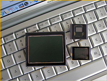
22 Megapixel 645 format
5 Megapixel 4/3 format
6 Megapixel 1/2.5 format
Imaging sensors come in different sizes, ranging from smaller than the nail on a baby’s pinky finger to almost the size of 645 format film. A sensor chip’s size is a key variable in determining its cost. Chips are made from silicon wafers. Whereas literally thousands of sensor chips, such as those used in a web cam, can be cut from a single wafer, only a handful of medium format chips can be derived from a standard 6"or 8" wafer. This means that their wholesale costs can range from less than a dollar, to more than $5,000 per finished chip.
The value of wafer real estate is just one factor in determining its cost. Rejection rate is another. With millions of components on a chip it’s almost impossible with today’s technology to make a perfect chip. (I was told by Dalsa, who made the sensor chips used in the Mars Rovers, that NASA had to test literally hundreds of chips till they found one that was perfect – and this was just a 1 Megapixel device). Consequently both manufacturers and camera makers set their own criteria for whether a chip is usable or not. This will include the number of defective pixels as well as rows, and consecutive rows that are permitted. The nature of these criteria are closely held corporate secrets.
Adding to the higher cost of these larger chips is that fact that the camera (back) makers will then create custom "profiles" for each chip, mapping its defects. This information is then burned into a ROM on each back, and this data is then copied into every raw file produced. When that file is processed by the maker’s raw processing software this "defect map" is then applied to the image data to compensate for these anomalies. Clearly this extra step is part of the high cost of medium format backs.
_________________________________________________________________
Pixel Size
Chip size and individual pixel size are factors which combine to determine not only a sensor’s cost but also many aspects of its performance. More pixels (photo sites) means higher resolution. But having more pixels to record ones images means either putting more of them on a chip, or making the chip bigger.
The only way to add more pixels to a chip of a given size is to make the pixels smaller. But, as the pixels become smaller they are less able to capture photons, and therefore their signal to noise ratio decreases. (All electronic circuits have inherent noise. The more signal (photons) there is, the lower the noise is relative to that signal).
This is a bit of a moving target. Chip makers and camera makers continue to improve their circuitry and noise reduction capabilities. But the laws of physics can’t be denied. And, any and all technologies used to reduce noise on new designs of chips with smaller pixels can equally be applied to those with larger pixels. So while absolute improvements are being seen, relatively speaking the gap between them remains roughly the same.
This is seen at the high end of the marketplace in the Kodak chips used in certain medium format backs. The 22 Megapixel chip used in the Phase One P25 has large 9 micron pixels. When introduced a few years ago these were considered to be essentially noise free at their native ISO of 50.
The 39 Megapixel chip used in the Phase One P45 back, introduced by Kodak in late 2005, uses 6.8 micron pixels – some 25% smaller. And yet Kodak claims an equivalent S/N, and this is backed up by users tests which show it to be the case.
Does this mean that we can expect to see ever increasing pixel densities? Maybe a bit. I’ve been told by some industry insiders that Kodak has indicated that it expects to be able to manufacture a 55 Megapixel 645 format sensor with equivalent S/N ratio within a couple of years. I haven’t done the math, but this likely means a pixel size of about 5 microns, which appears to be getting very close to the practical limits of what on-chip noise reduction technology can handle and still produce professional quality images.
_________________________________________________________________
The Laws of Physics
Visible light is found in the wavelengths between a 400-750nm (.4 to .75 micron). Obviously, an individual pixel (photo site) can’t be anywhere near this small and still record photons. Today’s smaller digicams feature sensors down to about 2.2 microns in size, and as we all know can be quite noisy. At this small size they simply can’t capture enough photons as compared with their inherent noise level. DSLRs offering 8-12 Megapixel on APS sized sensors seem, therefore, to have settled in the 5-6 micron level and offer an optimum combination of resolution, low noise and moderate cost.
In summary, if you try for ever higher resolution in a small chip –something’s gotta give. The smaller the pixels, the lower the quality as compared to a similar sensor with larger pixels. Very small pixels (sub 5 micron) start to run into the laws of physics, where signal to noise ratio, and the simple ability to capture enough photons limits their ability to sustain significant improvements given known technologies.
_________________________________________________________________
Making Sense of Sizes
So now we have enough information to try and make some sense of the entire issue of relative sensor size, image quality, and costs. Put simply –bigger is better, and costs more. That’s the core of any discussion about digital image sensors.
The statement that bigger is better has implications for the competitive marketplace. In the days of film no one argued with the fact that large format produced superior image quality to medium format, and that medium format offered higher image quality than 35mm, and so on down the food chain. (Issue of features, convenience, and size aside.)
This example holds true in much the same way today with digital. When enlarging medium format film, the fact that it required only a 4X enlargement to 35mm’s 8X to make a roughly similarly sized print gave MF a considerable advantage. Even with moderate sized prints the quality difference could be seen, as the demands on lenses were reduced.
With digital many argue that as long as an image doesn’t need to be enlarged beyond the resolving ability of the output medium (say, 300 ppi when making an inkjet print) there is no disadvantage to a smaller imaging chip. Well, maybe, but then, maybe not.
At first this seems like a sensible position to take, and when comparing mainstream DSLRs with say 8MP to 12 MP sensors, experiences shows it to be valid. But, this is not the case when the differences in sensor size are greater.
For example, one can take a file from a Canon 5D (13MP) and a Canon 1Ds MKII (16MP), and on just about any sized print one is hard pressed to tell the difference, especially when extraneous factors such as noise are excluded.
But when an 8MP DSLR such as the Canon 30D is compared to a 16 MP 1Ds MKII then there is a visible difference, almost regardless of print size. Or when a 5D is compared to a 22 MP camera or back, it is clearly visible, even when the print size is within reasonable limits. Why is this, and what are the factors contributing to what is being seen?
_________________________________________________________________
Like Falling off a Logarithm
Every photographer is familiar with the F stop scale, the ratio expressed logarithmically of a lens’ focal length to aperture. Each stop represents a doubling or halving of the amount of light reaching the sensor or film.
… F/2.8 – F/4 – F/5.6 – F/8 – F/11 – F16 – F/22 – F/32 – F/45 …
Similarly, going from a 6 Megapixel chip to a 11 Megapixel one doubles the number of pixels, and the F stop ratios are a convenient way of thinking about this. Is it any coincidence that standard F stop increments are very close to the Megapixel counts on chips? F/5.6 (6MP) to F/8 (8MP) is one stop – a doubling. F/11 (11MP) to f/16 (16MP) is another doubling.
But, as we all known from our personal experience, such an increase, a doubling of pixel count, doesn’t produce a doubling of apparent resolution. Subjectively what is seen is that such a doubling produces anoticeableincrease, but not a dramatic one. It isn’t until one increases pixel count by about two "stops" that an obvious advantage is shown by the larger chip. This is seen when going from a 6MP to an 11MP camera, or from a 16MP back to a 33MP or 39MP model. Simply put, it takes a quadrupling of area to produce a meaningful visible difference between sensors, even when both are being reproduced at the limits of the reproduction technology (say, 300 PPI on a print).
As to what these differences may be, we are now in the realm where bar room and discussion forum brawls break out. Some claim not to be able to see any significant differences under these circumstances. If so, fine, simply carry on as before. No one is trying to twist your arm. But, I can see the difference, and so can many other photographers.
What it is that we’re seeing is another matter. I describe it as micro-contrast; very fine tonal transitions that seems to get lost with smaller sizes. This could well be caused by the relative lack of strain on the camera’s lens when lower magnifications are called for. It is also something that we’ve always seen when comparing larger formats to smaller ones in the film world. Few would argue that a contact print from 8X10" film, or a 2X blow-up from 4X5" film, shows appreciably higher image quality than 35mm, even when both are printed well within the resolution limits of their optical train and the printing paper itself.
_________________________________________________________________
Plus ca change, plus c’est la meme chose
(The more things change, the more they are the same)
So – where does this all leave us? Well, maybe with enough information and empirical evidence we can derive a few practical rules of thumb. I’m therefore comfortable making the following generalizations based on today’s (2006) technology…
– sensors with photosites down to about 6.8 microns produce the highest quality, with little if any image quality degradation over ones with larger photo sites.
– sensors with pixels between about 5 microns and 6.8 microns are capable of excellent image quality, but are being pushed close to the limits of current technology when used at higher ISO settings, and suffer in this regard when compared with sensors with a larger pixel pitch.
– CMOS and CCD imagers will continue to share the market. More companies are moving to CMOS to reduce costs, but there are still new cameras coming to market using CCDs, and the high end of the market (medium format backs) continues to be the exclusive domain of CCD.
– physically larger sensors will always have an advantages over smaller ones. This means that (other factors aside) image quality from medium format will be higher than full-frame 35mm, which will be better than APS size, which will have an edge over 4/3, etc, etc.
– when upgrading from one camera to the next these factors should be borne in mind. Setting aside any other differences and advantages, be aware that unless you are making a "two stop" increase, it is unlikely that you will be excited by the difference in output or resolution seen. So, while a jump from a 6MP to a 12MP camera will be worthwhile, from a 6mp to an 8MP won’t, and neither will a jump from 16MP to 22MP.
_________________________________________________________________
Of course this article will be seen by some as fuel for not only interesting forum discussions, but also the usualmine is bigger (or better) than yourstype debates. I hope this piece to be a catalyst for the former, and express in advance my regrets if it acts as fuel for the latter.
The fact is that different tools address different market segments, and meet the needs of different photographic constituencies and shooting situations. For example, I currently am working with cameras with 5, 6, 8, 10, 13, 16 and 39 Megapixel chips. Each serves a specific purpose, and each has its strengths and failings. One size does not fit all.
August, 2006


Elevate Your Vision


Read this story and all the best stories on The Luminous Landscape
The author has made this story available to Luminous Landscape members only. Upgrade to get instant access to this story and other benefits available only to members.
Why choose us?
Luminous-Landscape is a membership site. Our website contains over 5300 articles on almost every topic, camera, lens and printer you can imagine. Our membership model is simple, just $2 a month ($24.00 USD a year). This $24 gains you access to a wealth of information including all our past and future video tutorials on such topics as Lightroom, Capture One, Printing, file management and dozens of interviews and travel videos.
- New Articles every few days
- All original content found nowhere else on the web
- No Pop Up Google Sense ads – Our advertisers are photo related
- Download/stream video to any device
- NEW videos monthly
- Top well-known photographer contributors
- Posts from industry leaders
- Speciality Photography Workshops
- Mobile device scalable
- Exclusive video interviews
- Special vendor offers for members
- Hands On Product reviews
- FREE – User Forum. One of the most read user forums on the internet
- Access to our community Buy and Sell pages; for members only.
You may also like