


Fig:1
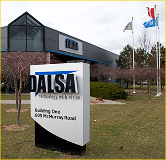
DALSA Head Office – Waterloo, Ontario
Interest in medium format digital is growing. The price of medium format backs is dropping, and untethered backs that can work in the field as easily as film backs are now available, or coming soon from all the major manufacturers. Mamiya has also recently shaken things up with their forthcoming 22 Megapixel ZD body and backs.
But, all of the companies making state-of-the-art 22 MP medium format backs use imaging chips from just two companies;KodakandDALSA. While DSLRs feature chips from Canon (who make chips only for their own cameras), Sony, Sanyo and Matsushita, who act as OEMs for just about everyone else, the makers of the very large and expensive chips for medium format are just these two.
____________________________________________________________________________________
Corn Fields
In an industrial park at the far north end of Waterloo, Ontario, is a campus of low-rise office buildings belonging to DALSA. Not more than a quarter mile away lies the rich farm land and corn fields of southwestern Ontario.
A strange location for a world-class high-tech firm? Not really. Waterloo is one of two high-tech centers in Ontario, Canada, the other being Kanata, one of the suburbs of Ottawa. The University of Waterloo is a primary reason, as it has long been one of Canada’s premier research centers, and the source of many of the county’s hi-tech entrepreneurs.
DALSA‘s corporate slogan isTechnology with Vision, most appropriate for a semiconductor designer and builder whose specialty is imaging chips; both CCD and CMOS designs. Though the company has been making industrial imagine chips for almost two decades, it was with the acquisition of Philips’ imaging chip division a few years ago that it expanded into chips for more traditional and high-end photographic applications.
DALSA continues to operate the previous Philips design center in Eindhoven, Holland, and also has their wafer fabrication plant in Bromont, Quebec, outside of Montreal.
____________________________________________________________________________________
Puff?
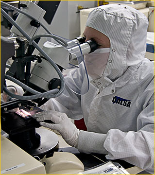
Fig 2.
Examining a Chip during manufacturing
This brief article isn’t intended to be either apuff pieceon DALSA, or an in-depth look at medium format chip design and manufacture. I don’t have the inclination for the former, or the knowledge for the later. But, an afternoon spent with Patrick Myles, DALSA’s Director of Corporate Communications, along with a tour of their head office, provided some insights into the current state of the industry.
A good place to start is to mention who DALSA currently makes 22 MP chips for. This includes Creo / Leaf, Jenoptik and Mamiya. Their competitor, Kodak, makes the chips used in medium format backs from Phase One, Imacon and Sinar.
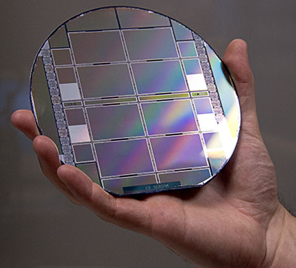
Fig 3.
A 6" wafer containing eight full-frame 35mm imaging chips
Just four 645 format chips can be made on a wafer this size.
Not all chips are usable, making yields much lower than production would suggest.
Something that I learned, which I didn’t know before, is that these very large chips are made up from 1K X 1K sub-components. This is unlike the much smaller chips, such as those up to APS-C size as used in DSLRs and digicams, which are made from one continuous die. The implication of this is that an imager of almost any size can be made, because these large chips are made from 1K X 1K components stitched together with firmware.
Below is a photograph of a 5,000 X 5000 pixel chip that is not used in any commercial camera. When asked who it was made for, and for what application, all I got was an enigmatic smile. Can you spellmilitary? Who else could afford it?
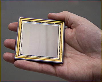
Fig 4
A 5K X 5K chip
These chips are all CCDs. But DALSA also makes CMOS chips for many applications, primarily industrial. When I asked about the pros and cons of each, one of the things that I was told is that a CMOS chip is much more expensive to design up-front, but then less expensive to manufacture, especially if quantities are high. The higher up-front costs include about a 4:1 ratio of design manpower over CCD, and also mask set costs that can run into the hundreds of thousands of dollars. But CMOS can also have greater on-chip support circuitry, such as noise reduction – which, incidently, it needs.
____________________________________________________________________________________
The Mamiya Factor
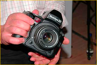
Fig 5
Mamiya ZD. Photo courtesy Mamiya Corp.
The 22 megapixel Mamiya ZD camera, along with their medium format backs for existing Mamiya cameras, first announced at Photokina in September, 2004, shook up the industry. Firstly, because they were unexpected, and secondly, because the ZD will likely have a retail price of well under USD $15,000 when it ships in the first quarter of 2005. This is half the price of current competitive 22 megapixel backs, let alone for a complete camera.
DALSA is the provider of the FTF4052C chip used in this ground-breaking camera. This was announced as a minimum $20 million contract for DALSA.
Now comes some speculation on my part. A couple of years ago I was told by an industry insider that 645 format 16 megapixel chips cost back makers about $5,000 a piece, in quantity. Given inevitable price reductions, but offset by an increase from 16MP to 22MP, it’s my guess that Mamiya is likely paying DALSA something like $3,000 a chip. This is mentioned just to give you a feel for what such large imaging chips cost, as compared to those in prosumer DSLRs, and goes a long way toward explain why such backs and cameras cost as much as they do.
Will these chips become even less expensive over time? Probably, but not that quickly. The problem is that volumes are low, and will likely remain low into the future. Canon probably makes more DSLR chips in a day, than 645 format chips from DALSA and Kodak combined in a year. No exaggeration.
____________________________________________________________________________________
To Mars
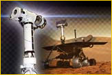
Fig. 6
DALSA fabricated the CCD chips that were used in the two Mars Rovers, based on a NASA design, in collaboration. These are still (Nov, 2004), photographing the surface of Mars. Apparently NASA took two years to certify the specific hand- picked chips used in the two Rovers. Talk about about yournit-picking pixel-peepers.
____________________________________________________________________________________
Origin
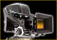
Fig. 7
Image courtesy DALSA
In addition to their medium format and industrial chips, DALSA also makes complete camera assemblies for industrial vision applications. But the most interesting complete camera is their newOrigindigital movie camera. If you’re interested, you can read more about it on the DALSA web site, and elsewhere. It is going to go into feature film production in just a few months. I saw the lab where these cameras are designed and built, and also viewed some sample footage. It was stunning in quality.
What makes this interesting is that unlike some of the high resolution digital cameras in use for the past year or two in Hollywood, used to produce features such as the lastStar Warsmovie, which used 3 CDD chips, similar to video camera design, the Origin uses a single 8 Megapixel chip the same size as a 35mm motion picture frame. This is a real plus for cinematographers, because it means that they are able to use all of their existing lenses. If you think that this isn’t a big deal, you’ve never worked with cinematographers, for whom their favourite lenses are their most prized tools. I spent several years working in the motion picture industry, and believe me, with their fastidiousness and attention to precision and detail these folks make neurotic photographers look like slovenly children.
In any event, this also means that lenses have their accustomed focal length, and therefore depth of field. Selective DOF is a huge issue issue for professional cinematography, and has been one of the impediments till now to the adoption of digital media for feature films.
The Origin system writes to a hard disk array at the speed of 400MB/Sec. These are RAW images, just like the raw files shot with still cameras. This means that they are processed similarly, though the processing power needed to handle such vast quantities of data is considerably greater than provided by your typical desktop Pentium.
The chip in the Origin uses a Bayer matrix, just like the CCD chips in almost all DSLRs and backs (Foveon excepted). For all its supposed drawbacks, Bayer is now a very mature technology, and especially with large chips, where there is a lot of data available, able to produce both highly accurate colour and resolution.
Another area in the motion picture industry where DALSA is active is with the sensor used to read the optical sound track on Dolby encoded motion pictures. Every theater projector in the world showing movies with a Dolby audio track uses a DALSA sensor chip.
____________________________________________________________________________________
Overall, a fascinating afternoon, and a small insight into a part of the photographic industry normally not open to view.
Photographs and Text Copyright 2004 – Michael H. Reichmann
Elevate Your Vision


Read this story and all the best stories on The Luminous Landscape
The author has made this story available to Luminous Landscape members only. Upgrade to get instant access to this story and other benefits available only to members.
Why choose us?
Luminous-Landscape is a membership site. Our website contains over 5300 articles on almost every topic, camera, lens and printer you can imagine. Our membership model is simple, just $2 a month ($24.00 USD a year). This $24 gains you access to a wealth of information including all our past and future video tutorials on such topics as Lightroom, Capture One, Printing, file management and dozens of interviews and travel videos.
- New Articles every few days
- All original content found nowhere else on the web
- No Pop Up Google Sense ads – Our advertisers are photo related
- Download/stream video to any device
- NEW videos monthly
- Top well-known photographer contributors
- Posts from industry leaders
- Speciality Photography Workshops
- Mobile device scalable
- Exclusive video interviews
- Special vendor offers for members
- Hands On Product reviews
- FREE – User Forum. One of the most read user forums on the internet
- Access to our community Buy and Sell pages; for members only.
You may also like