


On a cold but sunny day in late January, 2005, I drove from my home in Toronto to visit withEastman Kodak’s Image Sensor Solutions(ISS) division in Rochester, New York. It was my second visit in a couple of months with a major imaging chip designer and manufacturer. In the Fall of 2004 I had spent some time withDALSA, and my comments on that visit are online in an essay titledAn Afternoon with DALSA.
__________________________________________________________
Lack of Good Sources
The reason that I found visiting these companies of interest, is that there is little information publicly available about base level digital imaging technology. By way of anecdote, a while ago I was asked by a Japanese publisher for the use of some of my photographs in a forthcoming book. I agreed, and then promptly forgot about it. But a year later I received in the mail a copy of the book – a most wonderful text on digital imaging technology, loaded with great illustrations, diagrams, charts and graphs. That’s the good news. The bad news is that it’s entirely in Japanese. I’ve looked, but have been unable to find anything in English that has contemporary information for the intellegent layman, such as, for example, how microlenses work.
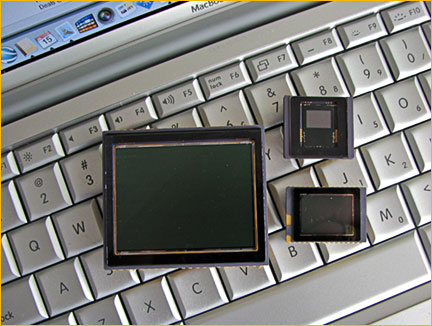
Illustration Courtesy Eastman Kodak
So, when I received an invitation from Kodak for an opportunity to meet with the folks that are responsible for making that company’s imaging chips, I was quick to respond. Who better to answer some of my questions than the proverbial horses mouth?
My hosts for this visit wereMichael DeLuca, Manager for Product Marketing, andManish Singh, the Product Development Engineer responsible for the Kodak sensors used in digital cameras and backs. Our meeting lasted for several hours, and in the end I left, not so much because I’d run out of questions, but because my mental RAM and notepad were overflowing.
Here then are some random observations and insights gleaned from this meeting. They’re not in any particular order, or importance, but are simply the things that I found to be of interest and which I wanted to know more about.
__________________________________________________________
Myth vs. Reality
Microlenses
Because of the lack of any good and readily available technical information on contemporary digital imaging base technology (at least that which is understandable by the layman), there is an amazing amount of misinformation and disinformation floating around the Net. One really has a hard time separating fact from fiction, or at least from partial truth.
One of these myths has to do with microlenses. I knew that their purpose was to better focus light onto the photosites, but why do some chips have them, and some don’t? How are they made? (I had visions of thousands of underpaid workers in a factory somewhere in China looking through microscopes and placing tiny little lenses on top of individual pixels) (Just kidding).
![]()
Diagram Courtesy Eastman Kodak
The purpose of microlenses is to better focus light down into the well where the light sensitive part of the photosite resides. Especially with wide angle lenses, light from the edges of the lens strikes the sensor at an acute angle, and therefore some of the light is lost against the sides of the well. A microlens focuses the light coming in at a sharp angle so that more of it hits the sensor at the bottom of the well.
How microlenses are made appears to be a bit of a trade secret, but it involves a transparent material which is coated onto the surface of the sensor. A pattern is etched onto this layer so that small “blocks” of this material remain over each pixel. The sensor is then baked so that the material “melts” to form small lenses over each pixel. The size of the “block”, the thickness of the deposited layer, and the surface tension of the material during the baking step all help determine the final shape of the microlens. Remarkable.
Microlenses aren’t used on all imaging chips. For example Kodak’s sensors that are currently used in medium format backs (such as the 22 million pixel KAF-22000CE, which has 9 micron pixels), does not use them, because while adding microlenses would increase the overallQuantum Efficiency(discussed later) of the sensor it would mean adding an additional optical element (the microlenses) to the system. The resulting sensor would not then be appropriate for use with swing / tilt lenses.
Noise and Pixel Size
One of the bits of common wisdom about pixel size is that larger pixels are less noisy. This is indeed true, but it is not so much that the pixels are “less noisy” but rather that they provide a larger dynamic range. All things being equal, a larger pixel can store more charge than a smaller pixel – so for a fully exposed image, the ratio of signal to noise (where noise is assumed to be constant here between the big and small pixels) would be greater with the bigger pixel.
For example, Kodak makes the sensors used inOlympusDSLRs. The pixels in the 5 Megapixel Olympus E1 are 6.8 microns, while those in the new E300 are 5.4 microns. But, two years have passed between the two generations of chips, and the already excellent noise characteristics of the E1 are retained in the E300, at least at lower ISO settings. This is due to changes in the physical design of the pixel used. For the KAF-8300CE, the chip used in the E-300, Kodak changed the physical architecture of the pixel so that it provided comparable imaging performance at the smaller pixel size.
It would seem that as time passes we can expect to see smaller chips with higher resolutions, all without much if any increase in noise, at least at base level ISO.
__________________________________________________________
Base ISO
Everyone knows that digital cameras have a "base level ISO" setting, the lowest sensitivity setting, at which noise is also lowest. But what we’ve seen is that sometimes different cameras which use the same chip have different base level ratings. Sometimes 50, 64 or 100. Why is this?
The answer partially lies in the fact that sensor makers like Kodak don’t publish an ISO spec. Rather, the talk aboutQuantum Efficiency (QE). This is a measure of how efficient the chip is in converting photons into electrons. It’s then up to the camera maker to apply their own electronics, which often includes both amplification and noise reduction circuitry, to achieve a desired ISO sensitivity.
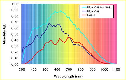
Diagram Courtesy Eastman Kodak
The diagram above shows how QE has improved over the past few years. The dark blue line shows QE from a Kodak chip (the one used in the DCS Pro Back). The dark blue line shows how the use of Kodak’s proprietaryIndium Tin Oxide(Blue Plus) technology produced much higher efficiency (and thus lower noise) in the blue channel, and then the light blue line shows the effect of adding microlenses. More than a doubling of QE at the critical 600nm wavelength. Note that the above chart presents QE for a monochrome device, not a color device (which would have separate QE curves for Red, Blue and Green).
__________________________________________________________
CCD Vs. CMOS
Up until recently Kodak primarily made CCD imaging chips. (The CMOS chip used in the unlamentedDCS 14nandPro n and cmodels is fromFill Factory). But over the past few years several Japanese companies proved that CMOS could be used to produce extremely high image quality, including notably Canon, and more recently Sony, which makes the CMOS chip used in the newNikon D2x.
Though CMOS chips are more complex and expensive to design, due to their built-in support electronics, they offer considerable cost advantages in terms of manufacturing cost and power consumption. Kodak is now moving to produce more of its own CMOS chips following its acquisition of theImaging GroupfromNational Semiconductor Corp.,which brings the company additional expertise and resources in this area. These chips will likely show up first in consumer digicams, a part of the market where Kodak’s digital camera division is currently one of the market leaders in North America. The cameras in mobile phones are also a huge potential market for Kodak.
__________________________________________________________
How Big Can Chips Get?
There have been rumours floating around the industry since Photokina in September, 2004, that we will see 38 Megapixel 645 format chips appearing in backs some time this year. While Kodak would neither confirm nor deny this (of course) it was an interesting exercise to do a little math in trying to determine how many Megapixels can be fit in the head of a pin, or at least into a 645 format chip.
If you take a 5.4 micron pixel size, which Kodak can now produce with very low noise, and make a 645 format chip, you end up with about 50 Megapixels. Is that as big as we’re likely to see? Who know? But certainly it’s completely possible with today’s technology. The real question is, who needs it? Especially the 300MB files that would be produced.
Illustration Courtesy Eastman Kodak
__________________________________________________________
Stitching
One of the things that surprised me when Ivisited Dalsawas that they claim to be able to make any sized chip, and that the reason this is so is because they stitch together 1K segments to whatever’s needed.
What I learned from Kodak was that they do not utilize this approach, but rather create complete unstitched chips of whatever size is needed using specialized silicon layout tools appropriate for the task. Apparently the advantage of this approach is that the segments don’t then need to be stitched together. A theoretical, if not actual, downside of stitching is that noncontiguous segments that are right next to each other will have slightly different characteristics, and therefore there is fine tuning of the signal that needs to be done to match levels. With a continuous design like that used by Kodak this is unnecessary.
The same issue applies to multiple read-outs off the chip. It is of course faster to read from two taps, but there are problems in matching the abrupt transitions between segments.
__________________________________________________________
The Future
No, Kodak didn’t divulge anything about future products, and yes I did ask. But it’s clear from a superficial overview of image chip making technology that these are still early days, and that we can expect to see faster, larger and cleaner chips in the months and years ahead.


Elevate Your Vision


Read this story and all the best stories on The Luminous Landscape
The author has made this story available to Luminous Landscape members only. Upgrade to get instant access to this story and other benefits available only to members.
Why choose us?
Luminous-Landscape is a membership site. Our website contains over 5300 articles on almost every topic, camera, lens and printer you can imagine. Our membership model is simple, just $2 a month ($24.00 USD a year). This $24 gains you access to a wealth of information including all our past and future video tutorials on such topics as Lightroom, Capture One, Printing, file management and dozens of interviews and travel videos.
- New Articles every few days
- All original content found nowhere else on the web
- No Pop Up Google Sense ads – Our advertisers are photo related
- Download/stream video to any device
- NEW videos monthly
- Top well-known photographer contributors
- Posts from industry leaders
- Speciality Photography Workshops
- Mobile device scalable
- Exclusive video interviews
- Special vendor offers for members
- Hands On Product reviews
- FREE – User Forum. One of the most read user forums on the internet
- Access to our community Buy and Sell pages; for members only.
You may also like